MacroFab utilizes a solder paste Jet Printer to help cut down the costs for our customers whenever we can. However, the minimum dot size it can print is 13mils. Due to this limitation a stencil may be required if the solder paste volume and/or paste dimensions are under these limits.
Jet Printer Specifications
Paste layer specifications that are below these limits will require the use of a solder paste stencil.
|
Property |
Value |
|---|---|
|
Minimum Paste Dot |
13mils (0.3302mm) |
|
Solder paste volume |
530mils³ |
|
Paste to Paste Clearance |
8mil (0.2032mm) |
Stencil apertures and Advanced Nano coating
Some design apertures are too small for the solder paste to properly be deposited with a stencil. We identify this using area ratios. If the Area ratio is less than 0.66, we will require the use of Advanced Nano coating to ensure the solder paste deposits on the PCB lands and does not adhere to the sidewalls. The use of Advanced Nano can allow us to print apertures with a area ratio as low as 0.55. If you have an aperture with an area ratio less than 0.55, we can revise the aperture design or stencil thickness to meet our requirements. 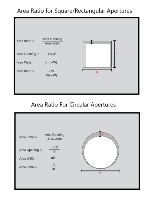
|
Property |
Value |
|
|---|---|---|
|
Standard Stencil Thickness |
4mils |
|
|
Minimum Aperture ratio (without Nano coating) |
0.66 |
|
|
Minimum Aperture ratio (with Nano coating) |
0.55 |
|
What is Advanced Nano coating?
Advanced Nano is a highly unique and patented coating that is applied to the bottom side of the stencil and inside the apertures, the squeegee side remains uncoated. This advanced coating provides the stencil with anti-adhesion properties. Advanced Nano stencil utilizes a specialized 1-2 um hardened nano coating. This permanent hydrophobic coating repels solder flux allowing increased transfer of paste. Advanced Nano Stencils improve solder paste deposits which results in consistent paste transfer volumes and minimizes bridges which leads to higher process stability with lower failure rates.