Working with the PCB Viewer
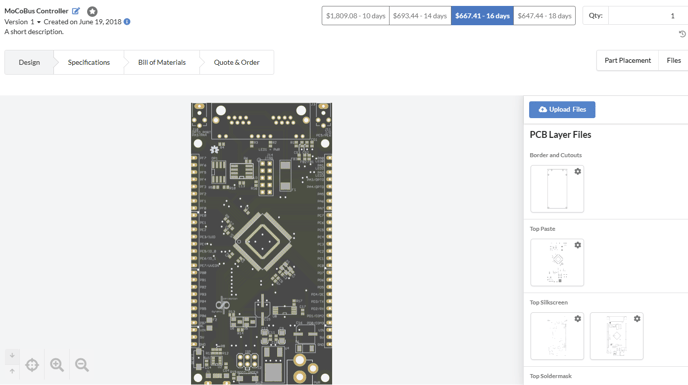
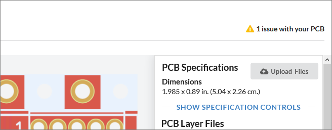
The Design tab of the PCB interface allows you to review your design files for correct alignment and check for mistakes before your order is processed. It also shows a render of your PCB of how it will look when manufactured. Changing the PCB’s soldermask color and silkscreen color will be reflected in the viewer in real-time.
The Design tab of the PCB interface allows you to review your design files for correct alignment and check for mistakes before your order is processed. It also shows a render of your PCB of how it will look when manufactured. Changing the PCB's soldermask color and silkscreen color will be reflected in the viewer in real-time.
Navigating in the Design Tab
PCB Layer List
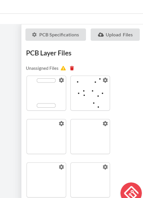
The PCB Layer Files list below the PCB Specifications section shows all the layers for the PCB. These are generated from the PCB gerbers or generated from the EDA file you uploaded. Hovering over a file with your mouse will show that file in the viewer if it is a PCB layer. 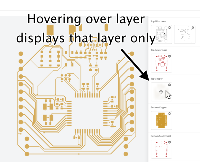
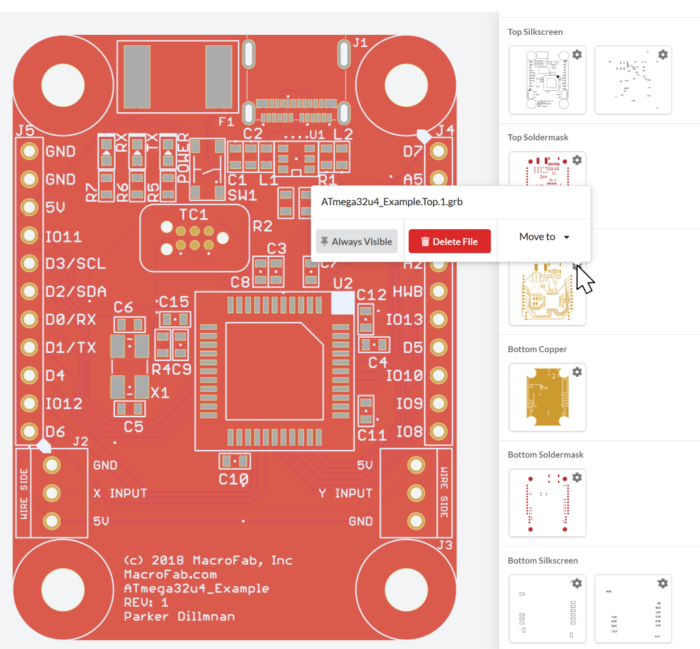
Hovering over the gear icon on the file will bring up a context menu for the layer. The menu will show the name of the layer and functions that allow deleting the file, pinning the file to be visible all the time, and moving the file to another layer. You can pin multiple layers at a time. Pinning layers turns the PCB viewer from a “realistic” render of the PCB to a gerber representation of the layer. You can also drag the layer to another section if you need to swap layers around!
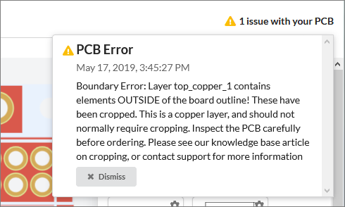
If the PCB you uploaded has problems with the layer files or processing issues you will see a yellow triangle in the upper right of the Design Viewer. This is where issues with your design files will be if there are any. Think of this as the DRC for your manufacturing files.
Hovering over the triangle will show all the issues. These should be carefully gone through as they can impact the success of your PCB Assembly. You can dismiss the error once you have resolved the problem or if the problem is fine.
Unassigned Files
If your manufacturing files uploaded to the MacroFab platform contain files that the platform does not recognize they will be placed in the Unassigned Files section of the PCB Layer List.
Rendering Issues and Other Concerns?
The PCB is shown using processed SVG files from the PCB data you upload, there may be artifacts displayed on the screen that show gaps in large pours that disappear when resizing or moving. These artifacts are caused by the SVG renderer in the browser and will not be present in your PCBs. Check our PCB Render Issues article to see if it is a common problem. If you have any questions or concerns with your PCB files or with how the PCB Viewer works in the platform contact our support team.
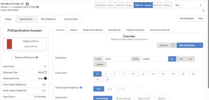
PCB Specification Controls
To advance to detailed PCB specifications, click the step tab labelled Specifications. For more information about customizing your PCB Specifications check out this article.