MacroFab Provides Several Standard Stackups as well as the option to create your own Stackup
With the advancement of modern electronics and miniaturization of products, the popularity of multilayer PCBs has grown. The PCB Stackup refers to the arrangement of copper layers, silkscreen, soldermask, and insulating layers that make up the PCB layout. This PCB Stackup has become more important as devices get smaller and faster as it is one of the most important parts in determining the Electromagnetic Compatibility (EMC) of the final product and PCB.
PCB Layer Stackups

MacroFab has a set of standard default PCB layer stackups for PCBs of layer 2 through 10. Due to the complexities of additional layers, we do not have a default stackup for PCBs more than 10 layers. Contact us if you need this information.
Multilayer PCBs consist of one or more layers of core and pre preg materials to isolate the copper layers from each other. The core material is a glass-reinforced copper-plated epoxy laminate sheet. This is an already cured FR4 material with a thin copper layer on it. Pre Preg is a reinforcing fabric that is pre-impregnated with the resin. This resin is an epoxy based system and is used as a glue to bind the PCB Stackup together.
MacroFab Data Sheets
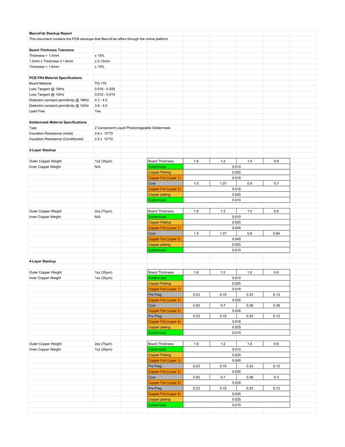
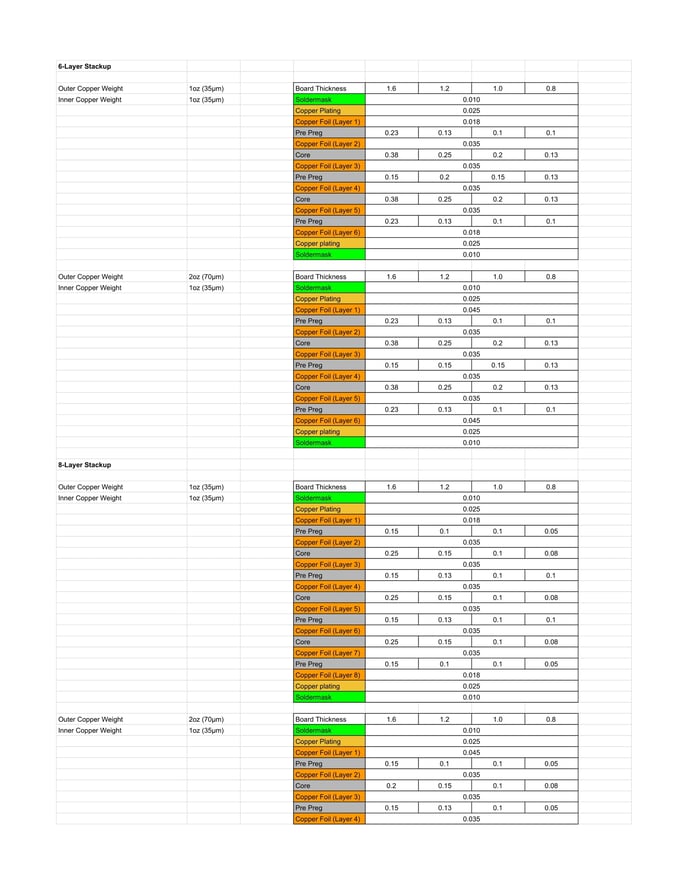
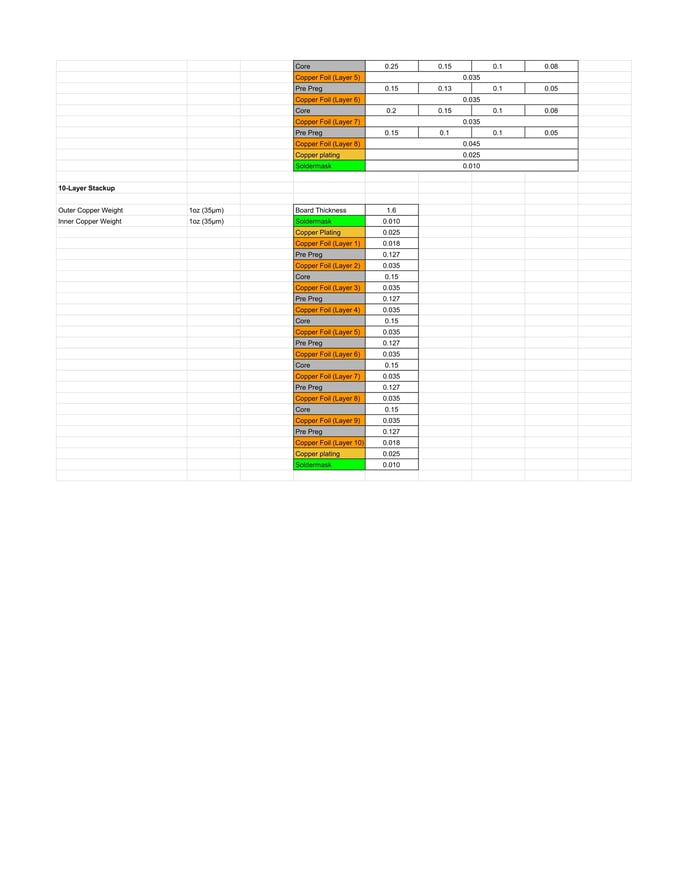
For PCBs that have 1oz (35μm) thick copper, you will notice that the Copper Foil layer and Copper Plating add up to over 35μm. This is due to the plating process when vias are added to the PCB. The IPC CLASS 2 PCB standard states that via wall plating needs to be a minimal of 0.8mil (0.02mm). The starting thickness of the copper foil is 0.5oz (18μm). After plating the copper foil the final thickness ends up in the range of 38μm to 43μm in thickness.
Stackup Related PCB Specifications
| Board Thickness Tolerance | |
|---|---|
| Thickness < 1.0mm | ± 15% |
| 1.0mm ≤ Thickness ≤ 1.6mm | ± 0.15mm |
| Thickness > 1.6mm | ± 10% |
| Minimum Board Thickness | |
|---|---|
| 2 Layer Boards | 0.2mm |
| 4 Layer Boards | 0.4mm |
| 6 Layer Boards | 0.6mm |
| 8 Layer Boards | 1.0mm |
| 10 Layer Boards | 1.0mm |
| 12 Layer Boards | 1.2mm |
| 14 Layer Boards | 1.4mm |
| 16 Layer Boards | 1.6mm |
| PCB FR4 Material Specifications | |
|---|---|
| Board Material | TG-170 |
| Loss Tangent @ 1MHz | 0.016 – 0.020 |
| Loss Tangent @ 1GHz | 0.012 – 0.014 |
| Dielectric constant permittivity @ 1MHz | 4.3 – 4.5 |
| Dielectric constant permittivity @ 1GHz | 3.8 – 4.0 |
| Lead Free | Yes |
| Soldermask Material Specifications | |
|---|---|
| Type | 2 Component Liquid Photoimageable Soldermask |
| Insulation Resistance (Initial) | 2.8 x 10¹³Ω |
| Insulation Resistance (Conditioned) | 2.5 x 10¹²Ω |
PCB Material Datasheets
Below you can find the datasheets for the materials that are used to create your PCB.
Click here to download an example FR4 Datasheet that meets our specifications
Click here to download the R-500 GHB Soldermask Datasheet
Custom PCB Stackups
In the PCB Specifications section of the Design Tab of the PCB interface, you can choose from a default set of standard stackups or specify custom stackups if your PCB Assembly requires it.
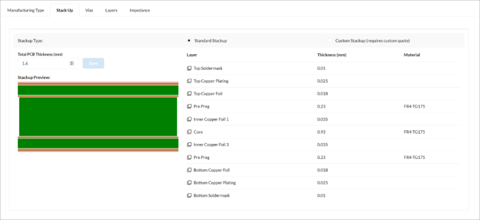
Custom stackups require a custom quote at this time and can not be instantly quoted through the platform.
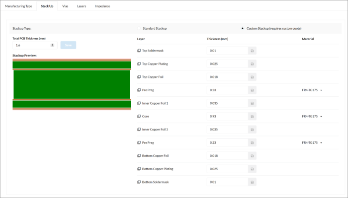
In the Custom stackup section, you can also specify the material used for your substrate. At this time FR4-TG175, Rogers 4003C, Rogers 4350B, and Rogers 4450B are supported in the platform. If you require material or a stackup that you can not define in the interface please let our support team know so we can get you a quote for your PCB Assembly right away.