The MacroFab platform looks for cutouts, plated slots, and other milling features in the .BOR or border layer of your PCB.
The MacroFab platform looks for cutouts, plated slots, and other milling features in the .BOR or border layer of your PCB. If your PCB has these features, they will need to be defined in the board outline layer in your EDA tool for the MacroFab platform to correctly render and manufacture the PCB. These are drawn in a similar fashion as the board outline is in most EDA tools. For more information on how to do this in your EDA tool check here. After uploading your files to the MacroFab platform you can check if your cutouts and plated sltos are correctly recognized by reviewing the Border Layer in the Design Viewer.
Check List for Valid Internal Cutouts and Plated Slots
- The line that defines the plated slot or cutout must not contain gaps, it should be a continuous line or “watertight”
- The line should be drawn on the perimeter of the route, one single "thick" line will not properly define the route
- Thickness of the line needs to be at least 1 mil
- Minimal route for internal cutouts and plates is 27mils (0.7mm) in width
Drawing Cutouts and Slots
For the below example, Eagle was used as the example EDA Tool. Other EDA tools should have similar mechanisms and tools to get the desired outcome. The plated slots required for a USB connector are drawn on the dimension layer for Eagle which is Layer 20. The plated slot is drawn using the line tool to denote the perimeter of the slot.
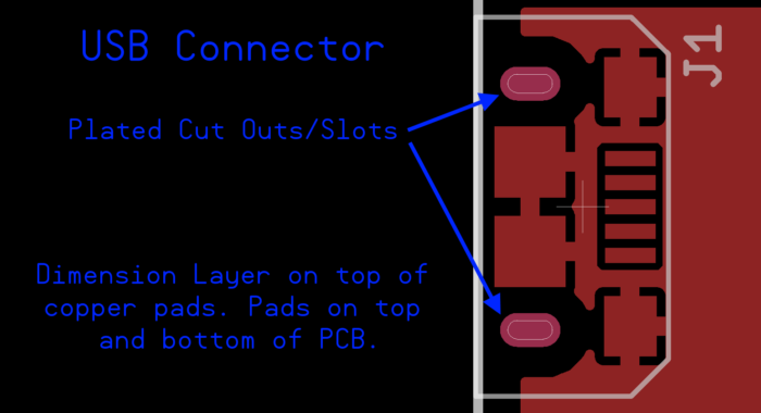
The edge of the plated slot and route will be determined by the center of the line. More information about this process can be found on the Board Outline article.
Invalid Methods of Drawing Cutouts and Slots
Using a Thick Line
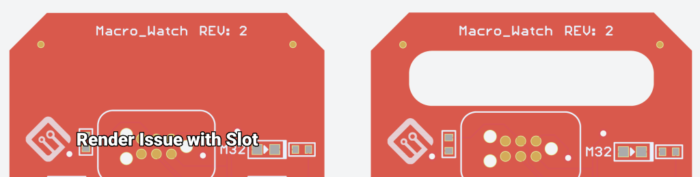
Drawing a cutout or slot with a single wide line won't give you the results needed and cause render issues in the platform. Routes need to be drawn showing the perimeter.
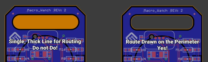
Routes drawn with a single thick line will not be rendered in the PCB Design Viewer correctly or may not render at all.
Putting Routes in the Excellon Drill File
Some EDA tools (Notably KiCad) will place plated slots and routes in the Excellon Drill File. This is known as the G85 drill command. MacroFab currently does not support this method to designate plated slots and routes. In the PCB Design Viewer a slot drawn in this manner will show up as two drill hits without a slot in between them. It is necessary to redraw the slot in a way that the EDA tool will export the slot as a feature of the border layer.
Non Plated or Plated Slots?
If you draw your cutouts/slots over copper it will be assumed to be a plated slot. This is similar to a drill placed in the center of a copper pad for a via. For non plated, pull the copper back at least the recommended distance from copper to board edge DRC. That is all you need to do to denote the difference between non plated and plated slots in your design files.
Questions about plated slots, cutouts, or internal routes?
Our support team is read to answer any question you can throw at them. Contact support today and help us improve our documentation!