The MacroFab platform requires a board outline gerber file to correctly manufacture your PCB.
This board outline gerber file is used to determine the extents of your PCB, calculate the size of your PCB, and remove excess features of your PCB that extend past this border. The PCB fab uses the board outline gerber file to route out your PCB and determine where slots and other cutouts should go.
Check List for Valid Board Outlines
- The line that defines the extent of the PCB must not contain gaps, it should be a continuous line or “watertight”
- Thickness of the board outline is atleast 1 mil
- Should not contain extra features outside of the pcbs extents
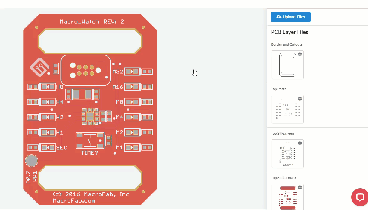
Board Outline In the PCB Viewer
In the MacroFab platform you can check your border file by using the PCB viewer. More information about how to use the viewer can be found in the Working with the Design Viewer article. The board outline layer should be checked to ensure it looks correct and that any cutouts or slots were captured.
Determining the Edge of your PCB
When the edge of the PCB is milled out of the FR-4 material (what PCBs are made out of) the PCB fab uses a round bit similar to a CNC machine. This causes the inside corners of the border of the PCB to have a round edge to them. This is something to watch out for in enclosure designs. The smallest tool used for routing out borders of PCBs is 1.0mm in diameter which means the smallest inside corner radius possible at MacroFab is 0.5mm. The tool cuts to the middle of the line regardless of the thickness of the line.
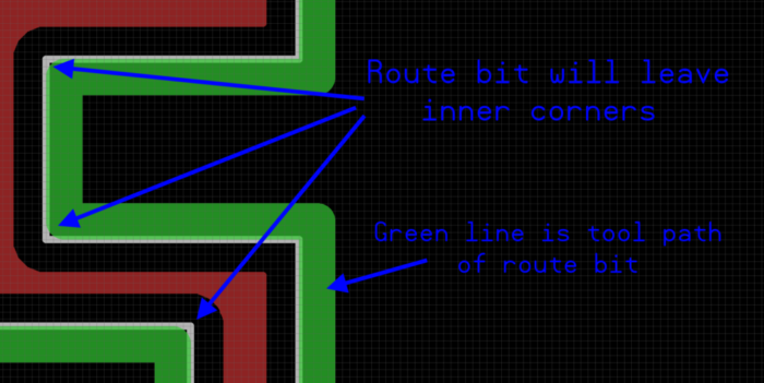 How the tool that cuts the border of your PCB routes. Green is the tool path. Grey is the board outline. Red is the copper layer.[/caption]
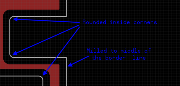 The tool that routes the edge of the board cuts up to the middle of the line. Due to the tool being round it leaves inside corners as rounded.[/caption]
Specifying Internal Corners
If your PCB has internal corners it is recommended to draw them in your EDA tool with a radius. Otherwise, the PCB manufacturer will specify the size of the radius that best fits there process. This might not be ideal if your PCB goes into an enclosure or has additional mechanical components that rely on a specific radius as the radius may change depending on the PCB manufacturer used.
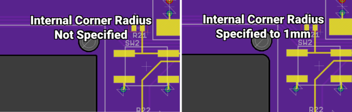
The best practice is to draw in the internal corners with a specified radius. The smallest tool used for routing out borders of PCBs is 1.0mm in diameter which means the smallest inside corner radius possible at MacroFab is 0.5mm.
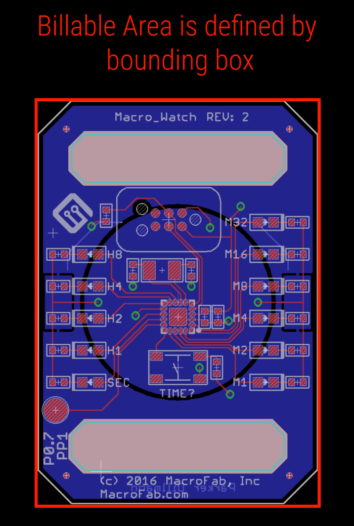
Calculating PCB Size
PCB dimensions are calculated from the bounding area of your PCB which is determined by the smallest rectangle that encloses your design. The smallest billable area is 1 sq inch or 25.4mm² so any boards smaller then this will be rounded up.
Plated slots and Other Milling Features
Any milling features, plated slots, or internal routes your PCB requires need to be included in the board outline for proper PCB manufacturing. See this article for more information.
Further Board Outline Questions?
Most EDA tools produce this necessary gerber file but if you need additional help in creating this file try our EDA tool help area of the knowledge base. If you think the border file is correct and the MacroFab platform is not recognizing or rendering it correctly, try the outline troubleshooting guide, or contact support so we can take a look at it.