Automated Manufacturing File Creation
In our mission to assemble your PCBs and ensure the highest quality while keeping your costs low, The MacroFab Platform is a fully automated process to convert the information about your PCB assembly and send it directly to our manufacturing lines. Additionally, by having all data about each order in our cloud systems, we are able to perform real-time optimization of orders by grouping together similar orders to reduce assembly line changes.
To facilitate this automated process, we need complete information about your PCB assembly. This includes PCB layer design files, bill of materials, and placement data for all components. These can be uploaded by dragging and dropping the file into our platform for instant quotes.
| EDA tool | PCB layer files | Component placement | Bill of Materials |
| Eagle | Board file .brd | ||
| KiCAD |
.kicad_pcb file |
.kicad_pcb file or .xlsx spreadsheet | |
| Altium, PADS |
ODB++ file, .zip, or .tgz |
Spreadsheet in .xlsx format | |
| DipTrace | Gerbers | ASCII file (.asc) | |
| Other | ODB++ | .XYRS or ODB++ | |
For supported EDA tools, we can extract this data automatically from the native files. Specific instructions on how to prepare your manufacturing files are available for the following supported EDA tools:
Is your favorite EDA tool not on this list? Let us know by contacting us. We are continuously working on instructions for new programs. If we don’t currently support or have specific instructions for your EDA tool, the following required design files are needed.
Required Design Files
To build your PCB assembly we will need three pieces of information: the layer information for the PCBs, a complete bill of materials, and where the parts will go on the PCB during assembly.
PCB Layer Files
PCB layer files are what tell the PCB manufacture where to put copper traces, drill holes, and apply silkscreen. Also included in the PCB layer files is a paste layer that tells the PCB assembler where to apply solder paste before the parts are applied.
There are two ways that MacroFab can accept PCB layer files: ODB++ output and Gerber Cam Files. The benefit of ODB++ is that it also contains a partial bill of materials and the placement data for your PCB. If your EDA tool supports ODB++ output this is your quickest way to getting a PCB created at MacroFab. However, not all EDA tools support ODB++ exporting. For those tools, you will need to generate the PCB layer files in the Gerber format.
ODB++ Output
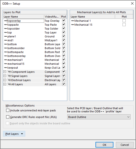
EDA tools that support ODB++ have a variety of options for data that can be packaged into the ODB++ output. Check to see if we have a guide for your specific EDA tool. If we do not, you will have to view the documentation for your EDA tool on how to operate the ODB++ generator. You will need to make sure the ODB++ output contains all relevant PCB Layer information and part placement information. Some EDA tools allow you to combine assembly or mechanical information with the layers. This causes problems during upload so make sure this is unchecked.

Gerber CAM files
Gerbers must be RS274-x format. If the following naming convention for the Gerber file extensions are used then the MacroFab platform will automatically associate the gerber file with the correct layer. The “pcbname” can be anything. The file extension is the only important part of the filename.
| PCB Layer | Gerber Extension |
|---|---|
| Top Copper | pcbname.GTL |
| Top Silkscreen | pcbname.GTO |
| Top Soldermask | pcbname.GTS |
| Top SMD Paste | pcbname.GTP |
| Bottom Copper | pcbname.GBL |
| Bottom Silkscreen | pcbname.GBO |
| Bottom Soldermask | pcbname.GBS |
| Bottom SMD Paste | pcbname.GBP |
| Board Outline | pcbname.BOR |
| Inner signal layers (postive polarity) – only used for multi-layer | pcbname.G2L, pcbname.G3L, pcbname.G4L, pcbname.G5L, pcbname.G6L, pcbname.G7L, pcbname.G8L, pcbname.G9L, pcbname.G10L, ect.. |
| Inner plane layers (negative polarity) – only used for multi-layer | pcbname.G2P, pcbname.G3P, pcbname.G4P, pcbname.G5P, pcbname.G6P, pcbname.G7P, pcbname.G8P, pcbname.G9P, pcbname.G10P, ect.. |
| NC Drill File (Excellon) | pcbname.XLN |
The above file naming format is suggested but not required. If the platform can not automatically identify the layer the file belongs to, you will be able to specify its location manually in the Design Viewer.
All cutouts and mills are required to be in the board outline gerber file.
Do not use a drill report or rack definition for the NC Drill File, this must be an included inside the NC Drill File.
Make sure to double check your inner layers for polarity. Generally EDA tools will export “plane” internal layers a negative polarity.
The board outline file is required for every PCB and should have an outline of the outer edges of the PCB. All drawings outside of this outline on other layers will be cropped.
Bill of Materials
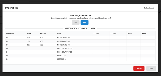
If you properly configured your ODB++ generator and uploaded it to the platform, a partial Bill of Materials will be filled out for your PCB. You can use our interactive Bill of Materials manager to complete the Bill of Materials or you can upload a spreadsheet in .XLSX format. The knowledge base article Importing a Bill of Materials Spreadsheet covers how this process works. Designators in your Bill of Materials will need to be unique.

BOM File
Here is a sample BOM with the required Column Headers. Note - to DNP enter 0 for each designator you would like to not populate. Sample BOM
Component Placement Files
The last piece of information MacroFab needs to build your PCB is the component placement information. If you are using a supported EDA tool this information is easily extracted during the upload process automatically! A properly configured ODB++ output will also contain the component placement information. If your EDA tool is not supported and does not support the ODB++ generation then you will need to build your component placement information by hand in the form of the .XYRS format.
.XYRS File Format
The .XYRS format is a combined Bill of Material and XYRS data file that is used to place parts on the PCB. The file should have the extension “.XYRS”. The file is tab delimited and should contain the following fields. All the dimensions are in mils for X-Y locations and X-Y part size. Rotation is in degrees.
Lines beginning with ‘#’ will be ignored
| Column | Description | Example |
|---|---|---|
| Designator | Part Name | U1, R10, C8 |
| X-Loc | X-Location of Part (mils, oriented from bottom-left) | 1200.00 |
| Y-Loc | Y-Location of Part (mils, oriented from bottom-left) | 900.00 |
| Rotation | Rotation of Part (degrees) | 270 |
| Side | Layer the Part is On | 1/T/top for Top, 2/B/bot/bottom for Bottom |
| Type | Surface or Through Hole | 1/SMT/SMD for SMD, 2 for PTH |
| X-Size | X Dimension of the Part (mils) | Size of the Package, Measured By the Pad Footprint |
| Y-Size | Y Dimension of the Part (mils) | Size of the Package, Measured By the Pad Footprint |
| Value | Value of Part | 10K, 0.1uF, ATMEGA328P-AU |
| Footprint | Footprint of Part | C0805, R0603, TQFP-100 |
| Populate (optional) | Whether or not to populate this part | 1 for populate, 0 for do not populate |
| MPN (optional) | The MPN for this part | MF-CAP-0402-27pF |
An example line from a .XYRS file should look like the following.
| Part | X | Y | Rotation | Side | Type | XSize | YSize | Value | Footprint | Populate | MPN |
|---|---|---|---|---|---|---|---|---|---|---|---|
| R1 | 1200.00 | 900.00 | 180 | 1 | 1 | 40.0 | 20.0 | 1K | 0402-RES | 1 | MF-CAP-0402-27pF |
An example .XYRS file can be found here.
A note about uploading .XYRS files to an existing Bill of Materials (BoM):
Uploading an .XYRS file to an existing BoM is a merge operation. First, the existing BoM is pulled. The part origins, alternative parts lists, and components of alternative parts lists are captured. Second, this existing data is merged into the newly uploaded .XYRS file.
These are the rules that govern the merge:
- If the newly uploaded .XYRS file has a designator that existed in the old BoM, the origin will always be copied from the old BoM (even if the MPN is different) onto the new BoM.
- Please note for consignment: If the MPN matches, the consignment configuration (pin count, mount type) will be transferred, but if the MPN doesn't match, the configuration must be manually defined.
- If the newly uploaded .XYRS file has a designator that existed in the old BoM, and the MPN in the new .XYRS file is in the alternative parts list for the old BoM designator row, this alternative parts list will persist onto the new BoM. If the MPN in the new .XYRS file is not in the existing alternative parts list, then the existing alternative parts list will be overwritten.
- If the newly uploaded .XYRS file has a designator not found in the old BoM, the designator is added as defined in the new .XYRS file.
- If the old BoM has a row not represented in the new .XYRS file, it will be removed.
This behavior ensures that a user can download an .XYRS file from their PCB, change a single row's MPN, origin, or placement, and all of the other (unchanged) parts will be completely unaffected.
Support
If you have any questions on what kind of information you need to get your PCB ordered or looking for help with your specific EDA tool please contact our support team.